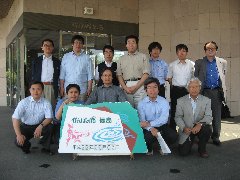
1. Convener: Dr. Kenjiro Nishikawa, NTT Network Innovation Laboratories, NTT Corporation
2. Date/time: 13:30 - 18:00, 4-June.-2010
3. Venue: Tokushima University, Tokushima, Japan
4. Registration fee: Free
5. Listed attendees: 29 persons
6. Local arrangement: Prof. Yasuo Ohno (Tokushima University)
7. Session title: "High-speed/High frequency Packaging and Board Design Techniques"
8. Presentation: 50 min including Q&A for each speaker
9. Reception and Lamp Session at Kanpo-no-yado Tokushima, Tokushima, Japan. Banquet
10. The steering committee meeting took place from 08:00 to 9:00 on 5-June-2010
11. Concluding Remarks
This workshop was entitled "High-speed/High frequency Packaging and Board Design Techniques " and had three talks. Design techniques for high-speed board and millimeter-wave highly-integrated packaging with antennas were discussed. Tutorial talk for GaN power device was also presented. In the lamp session, we deeply discussed two-dimensional FD-TD method for analysis of planar circuits
 1. Convener: Dr. Kenjiro Nishikawa, NTT Network Innovation Laboratories, NTT Corporation
 ホームへ戻る 日本学術会議 URSI-C小委員会